In the high-stakes world of military and defense operations, where failure is not an option, Printed Circuit Boards (PCBs) form the backbone of countless electronic systems. From radar control to communication devices, these compact powerhouses enable everything from unmanned drones to satellite navigation. But what ensures these PCBs perform flawlessly under extreme conditions like scorching heat, intense vibrations, or electromagnetic interference? The answer lies in specialized defense PCB test equipment. This blog dives deep into the importance, types, standards, challenges, and future of testing equipment tailored for defense applications, shedding light on how it safeguards national security.
Understanding PCBs in Defense Contexts
PCBs in defense aren’t your everyday circuit boards found in consumer gadgets. They must endure harsh environments, including temperatures exceeding 150°C, high-altitude pressures, and constant mechanical stress. According to industry experts, military PCBs are engineered with high-temperature laminates, copper, or aluminum substrates to resist oxidation and dissipate heat efficiently. Applications span a broad spectrum: power supplies for Airborne Warning and Control Systems (AWACS), auxiliary units for radar, radio communications, LED lighting, underwater navigation, jet instrumentation, jamming systems, and even firearms and explosives testing equipment. These boards power critical missions, where a single fault could compromise lives or operations.
The demand for reliability drives the need for rigorous testing. Defense PCBs often incorporate advanced designs like High-Density Interconnects (HDI) for compact circuitry in drones or night vision gear, or rigid-flex types to reduce wiring in portable military equipment. Testing ensures these innovations don’t falter in the field.
Key Types of Defense PCB Test Equipment
Testing defense PCBs involves a suite of sophisticated equipment, each targeting specific aspects of functionality, durability, and compliance. Here’s a breakdown of the primary types:
1. In-Circuit Testing (ICT): This method uses a bed-of-nails fixture to probe individual components on the PCB, checking for shorts, opens, resistance, capacitance, and diode functionality. In defense, ICT is crucial for high-volume production of boards used in missile detection or control systems, ensuring zero defects before deployment. It’s fast and accurate but requires custom fixtures, making it ideal for standardized military hardware.
2. Flying Probe Testing: A non-fixture alternative, flying probes move dynamically across the board to test electrical performance. This is particularly useful for prototypes or low-volume defense PCBs, like those in custom jamming systems. It detects manufacturing defects without physical contact damage, and equipment like advanced flying probe machines can handle complex multi-layer boards.
3. Automated Optical Inspection (AOI): Using high-resolution cameras and AI algorithms, AOI scans for visual defects like solder bridges, missing components, or misalignment. In aerospace defense, where PCBs face vibrations from jet engines, AOI verifies assembly quality at each manufacturing step. It’s non-contact and rapid, often integrated with X-ray for deeper insights.
4. X-Ray Inspection: For hidden defects in Ball Grid Arrays (BGAs) or multi-layer boards, X-ray equipment reveals voids, cracks, or poor solder joints. Defense applications, such as satellite equipment, rely on this to ensure integrity under radiation or thermal cycling.
5. Functional Testing: This simulates real-world operation, powering the PCB and verifying outputs against specifications. In military contexts, it might involve testing radio communication boards under simulated battlefield interference.
6. Burn-In Testing: Boards are subjected to elevated temperatures and voltages to accelerate aging, weeding out early failures. Essential for long-endurance systems like unmanned vehicles, this ensures reliability over extended missions.
7. Electromagnetic Compatibility (EMC) Testing: Defense electronics must resist jamming or emissions. EMC equipment tests for susceptibility to electromagnetic pulses, crucial for electronic countermeasures.
8. Strain Gauge Testing Kits: These measure mechanical stress on PCBs, complying with standards like IPC/JEDEC 9704. Kits include tools for applying and monitoring strain, vital for boards in high-vibration environments like firearms testing.
9. Microsectioning Systems: For destructive analysis, these cut and polish PCB cross-sections for microscopic examination of internal structures. Equipment like electronic microscopes with 40x magnification helps detect delamination or plating issues in defense labs.
10. Environmental Test Chambers: Though not exclusive to PCBs, these simulate extreme conditions like humidity, salt fog, or shock, ensuring defense boards meet MIL-STD requirements.
These tools collectively form a robust testing ecosystem, often automated for efficiency in high-stakes production.
Standards and Certifications Governing Testing
Defense PCB testing adheres to stringent standards to guarantee performance. Key ones include MIL-PRF-31032 and MIL-PRF-55110, which mandate monthly group A testing on aspects like solderability, ionic contamination, plating adhesion, and electrical continuity. Isolation resistance must exceed 10 mΩ, with voltage tests at 40V or higher. Certifications like ITAR, AS9100D, and IPC Class 3/ES ensure compliance for DoD criteria. Manufacturers provide full traceability, including first article inspection reports and cross-section analyses.
Challenges in Testing Defense PCBs
Testing isn’t without hurdles. Extreme conditions demand equipment that can handle high pressures and temperatures without compromising accuracy. Supply chain issues for specialized materials, like radiation-hardened substrates, complicate prototyping. Miniaturization increases complexity, requiring finer probes and higher-resolution imaging. Cybersecurity threats in connected test systems add another layer, necessitating secure protocols.
Cost is a factor; advanced equipment like X-ray machines or EMC chambers requires significant investment, but the payoff in mission success is invaluable.
Future Trends in Defense PCB Test Equipment
Looking ahead, AI and machine learning will revolutionize testing, predicting failures through data analytics. Integration of 5G and IoT in defense will demand enhanced EMC tools. Additive manufacturing for PCBs could introduce new test methods, like in-situ monitoring during printing. Sustainability pushes for eco-friendly testing, reducing waste in microsectioning.
Quantum computing might simulate PCB behavior, minimizing physical tests. As conflicts evolve with cyber elements, test equipment will focus more on resilience against digital attacks.
Conclusion
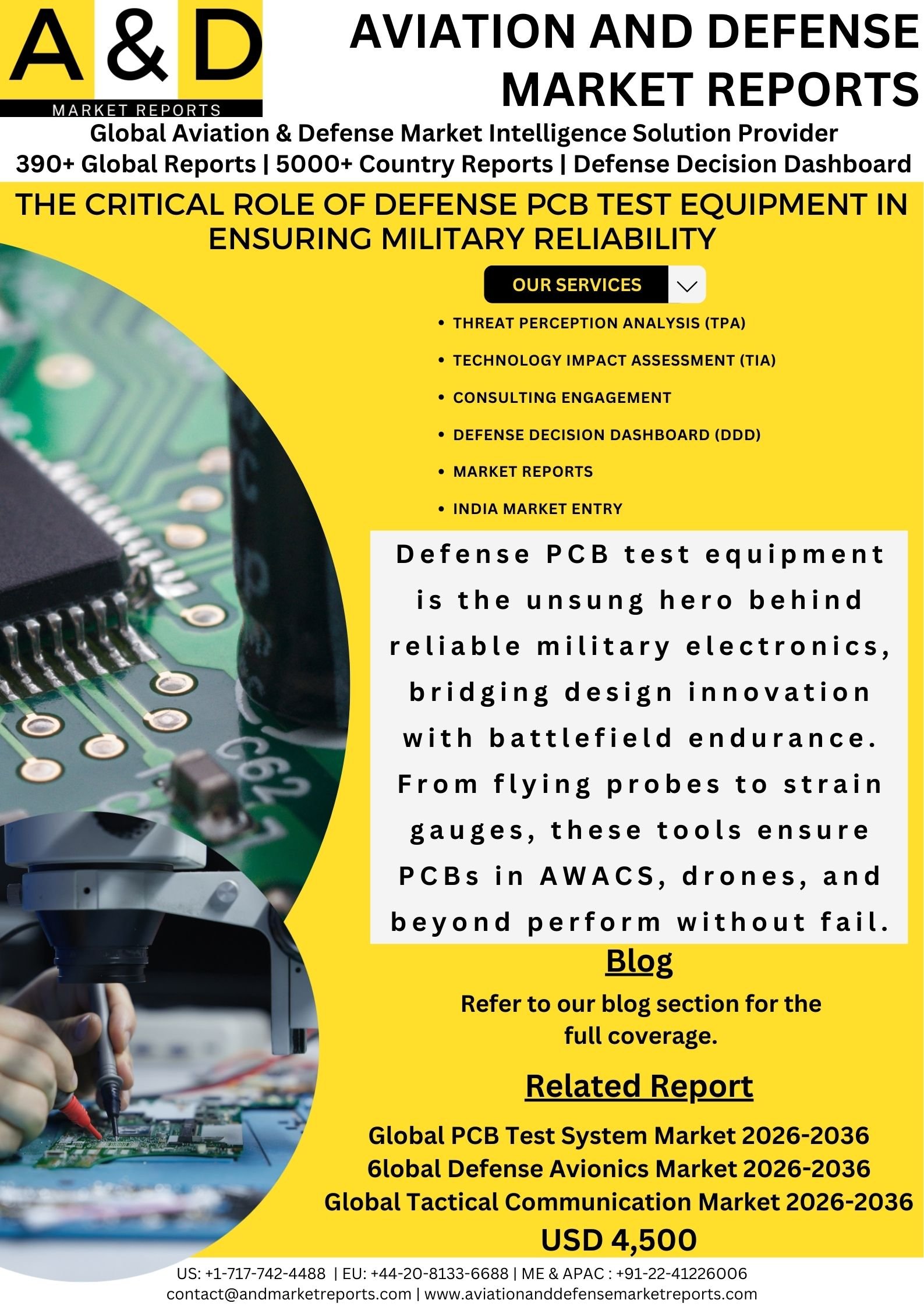
Defense PCB test equipment is the unsung hero behind reliable military electronics, bridging design innovation with battlefield endurance. From flying probes to strain gauges, these tools ensure PCBs in AWACS, drones, and beyond perform without fail. As technology advances, so will testing methodologies, keeping defense forces one step ahead. In a world where precision saves lives, investing in top-tier test equipment isn’t just smart—it’s essential.